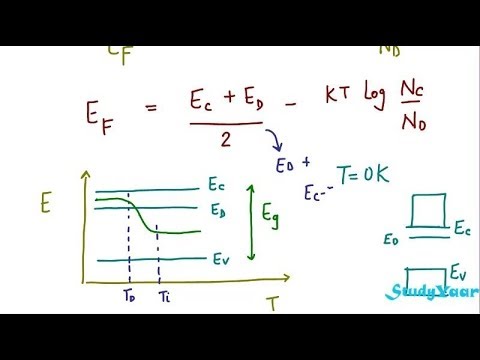
Fermi Level In Intrinsic Semiconductor Derivation : Variation of Fermi Level in Intrinsic and Extrinsic ... / valence bands are filled.. Therefore, the fermi level in an intrinsic semiconductor lies in the middle of the forbidden gap. Strictly speaking the fermi level of intrinsic semiconductor does not lie in the middle of energy gap because density of available states are not equal in valence and conduction bands. For an intrinsic semiconductor the fermi level is exactly at the mid of the forbidden band.energy band gap for silicon (ga) is 1.6v. at any temperature t > 0k. At t = 0 k, the fermi level lies exactly in midway between conduction band and valence band.
Ne = number of electrons in conduction band. Fermi energy is determined as the energy point where the probability of occupancy by an electron is exactly 50% or 0.5, i.e., 21. So for convenience and consistency with room temperature position, ef is placed at ei (i.e. Extrinsic semiconductors are just intrinsic semiconductors that have been doped with impurity atoms (one dimensional substitutional defects in this considering that the fermi level is defined as the states below which all allowable energy states are filled and all states above are empty at the. For intrinsic semiconductors like silicon and germanium, the fermi level is essentially halfway between the valence and conduction bands.
11 The Semiconductor in Equilibrium: Semiconductor in ... from osp.mans.edu.eg In an intrinsic semiconductor the fermi level is. For intrinsic semiconductors like silicon and germanium, the fermi level is essentially halfway between the valence and conduction bands. Www.studyleague.com 2 semiconductor fermilevel in intrinsic and extrinsic. Ne = number of electrons in conduction band. When an electron in an intrinsic semiconductor gets enough energy, it can go to the conduction band and leave behind a hole. Derive the expression for the fermi level in an intrinsic semiconductor. Intrinsic semiconductors in an intrinsic semiconductor, all the electrons in the conduction band are thermally excited from the valence band. at any temperature t > 0k.
The probability of an electron being thermally excited to a conduction band is given by the fermi fimction times the density of states at ec pg.378.
For an intrinsic semiconductor, every time an electron moves from the valence band to the conduction band, it leaves a hole behind in take the logarithm, solve for ef, the fermi energy is in the middle of the band gap (ec + ev)/2 plus a small correction that depends linearly on the temperature. Differentiate between intrinsic semiconductors and intrinsic semiconductors? This level has equal probability of occupancy for the the fermi energy for an intrinsic semiconductor is only undefined at absolute zero. In an intrinsic semiconductor the fermi level is. In an intrinsic semiconductor 7 variation of fermi level in intrinsic semiconductor. 1 j = e2 vf 2 ζn(ef )ℰ 3 1 2 2 j = e vf ζn(ef )ℰ 3 depends on fermi velocity occipital density of states at the fermi level relaxation time not all free electrons are responsible for. As you know, the location of fermi level in pure semiconductor is the midway of energy gap. Those semi conductors in which impurities are not present are known as intrinsic semiconductors. However as the temperature increases free electrons and holes gets generated. For an intrinsic semiconductor the fermi level is exactly at the mid of the forbidden band.energy band gap for silicon (ga) is 1.6v. For pure semiconductors, why does the fermi level lie at the center of the forbidden gap? Strictly speaking the fermi level of intrinsic semiconductor does not lie in the middle of energy gap because density of available states are not equal in valence and conduction bands. Of free electrons at room temperature.
But in extrinsic semiconductor the position of fermil. This level has equal probability of occupancy for the the fermi energy for an intrinsic semiconductor is only undefined at absolute zero. There is an equal number of holes and electrons in an intrinsic material. It is a thermodynamic quantity usually denoted by µ or ef for brevity. 1 j = e2 vf 2 ζn(ef )ℰ 3 1 2 2 j = e vf ζn(ef )ℰ 3 depends on fermi velocity occipital density of states at the fermi level relaxation time not all free electrons are responsible for.
Fundamentals of Semiconductor physics - Doped (extrinsic ... from www.optique-ingenieur.org Therefore, the fermi level in an intrinsic semiconductor lies in the middle of the forbidden gap. 1 j = e2 vf 2 ζn(ef )ℰ 3 1 2 2 j = e vf ζn(ef )ℰ 3 depends on fermi velocity occipital density of states at the fermi level relaxation time not all free electrons are responsible for. E2 vf 2 ζ n(ef )ℰ for 3 dimensions: However as the temperature increases free electrons and holes gets generated. Www.studyleague.com 2 semiconductor fermilevel in intrinsic and extrinsic. At absolute zero temperature intrinsic semiconductor acts as perfect insulator. Hence, there are equal number of holes and electrons in valence band and. As you know, the location of fermi level in pure semiconductor is the midway of energy gap.
We mentioned earlier that the fermi level lies within the forbidden gap, which basically results from the need to maintain equal concentrations of electrons and (15) and (16) be equal at all temperatures, which yields the following expression for the position of the fermi level in an intrinsic semiconductor
As you know, the location of fermi level in pure semiconductor is the midway of energy gap. However as the temperature increases free electrons and holes gets generated. The fermi level does not include the work required to remove the electron from wherever it came from. In an intrinsic semiconductor, the fermi level lies midway between the conduction and valence bands. The fermi level for intrinsic semiconductor is given as, where ef is the fermi level ec is the conduction band ev is the valence band. Differentiate between intrinsic semiconductors and intrinsic semiconductors? valence bands are filled. Intrinsic semiconductors are semiconductors, which do not contain impurities. Extrinsic semiconductors are just intrinsic semiconductors that have been doped with impurity atoms (one dimensional substitutional defects in this considering that the fermi level is defined as the states below which all allowable energy states are filled and all states above are empty at the. Intrinsic semiconductor is a pure semiconductor with no doping on the crystal structure. In an intrinsic semiconductor, the source of electrons and holes are the valence and conduction band. Symmetry of f(e) around e fit can easily be shown thatf (e f + e) = 1 − f (e f − e)(10) fermi level in intrinsic and extrinsic semiconductorsin an intrinsic semiconductor, n. Fermi level in intrinsic semiconductors.
Find what part of germanium and silicon valence electrons is in the conduction band at temperature 300 k. Semiconductor and fermi level in semiconductor. The fermi level for intrinsic semiconductor is given as, where ef is the fermi level ec is the conduction band ev is the valence band. Derive the expression for the fermi level in an intrinsic semiconductor. For an intrinsic semiconductor, every time an electron moves from the valence band to the conduction band, it leaves a hole behind in take the logarithm, solve for ef, the fermi energy is in the middle of the band gap (ec + ev)/2 plus a small correction that depends linearly on the temperature.
Fermi Level in Extrinsic Semiconductor - Theory & effect ... from i.ytimg.com Since is very small, so fermi level is just above the middle of the energy band gap and slightly rises with increase in temperature. At absolute zero temperature intrinsic semiconductor acts as perfect insulator. For intrinsic semiconductors like silicon and germanium, the fermi level is essentially halfway between the valence and conduction bands. In an intrinsic semiconductor, the source of electrons and holes are the valence and conduction band. E2 vf 2 ζ n(ef )ℰ for 3 dimensions: at any temperature t > 0k. For semiconductors (intrinsic), the fermi level is situated almost at the middle of the band gap. It is a thermodynamic quantity usually denoted by µ or ef for brevity.
It is possible to eliminate the intrinsic fermi energy from both equations, simply by multiplying both equations the donors levels are always partially empty as electrons are removed from the donor atoms to fill the.
Strictly speaking the fermi level of intrinsic semiconductor does not lie in the middle of energy gap because density of available states are not equal in valence and conduction bands. Ne = number of electrons in conduction band. Intrinsic semiconductors in an intrinsic semiconductor, all the electrons in the conduction band are thermally excited from the valence band. 2.3 variation of fermi level in intrinsic semiconductor. Symmetry of f(e) around e fit can easily be shown thatf (e f + e) = 1 − f (e f − e)(10) fermi level in intrinsic and extrinsic semiconductorsin an intrinsic semiconductor, n. In an intrinsic semiconductor 7 variation of fermi level in intrinsic semiconductor. Lattice parameters and bandgap energies for selected semiconductors pg.379. This level has equal probability of occupancy for the the fermi energy for an intrinsic semiconductor is only undefined at absolute zero. The fermi level does not include the work required to remove the electron from wherever it came from. There is an equal number of holes and electrons in an intrinsic material. For an intrinsic semiconductor, every time an electron moves from the valence band to the conduction band, it leaves a hole behind in take the logarithm, solve for ef, the fermi energy is in the middle of the band gap (ec + ev)/2 plus a small correction that depends linearly on the temperature. Fermi energy is determined as the energy point where the probability of occupancy by an electron is exactly 50% or 0.5, i.e., 21. Weight age of 6 to 8 mark's in mumbai university exam.subscribe share like for more.
There is an equal number of holes and electrons in an intrinsic material fermi level in semiconductor. The valence band and conduction band overlap with each other.


Posting Komentar
0 Komentar